Specifications:
| Materials | Silicon crystals | Diameter Range | ~300mm |
| Diameter Tolerance | -0.01/-0.03mm | Thickness Tolerance | +/-0.03mm |
| Surface Quality | 60/40 S/D | Frings (N) | 3 |
| Irregularity (delta N) | 1 | Centration | 3' |
| Chamfer | 0.1-0.3mmx45 degree | Coatings | AR/AR@3-5micro DLC/AR@3-5micro |
Physical and Optical Properties:
| Transmission Range | 0.12μm to 15 μm and and 30μm to >100 μm (1) | Refractive Index | 3.4223 @ 5 μm (1) (2) |
| Reflection Loss | 46.2% at 5 μm (2 surfaces) | Absorption Coefficient | 0.01 cm-1 at 3 μm |
| Reststrahlen Peak | n/a | dn/dT | 160 x 10-6 /°C (3) |
| dn/dμ = 0 | 10.4 μm | Density | 2.33 g/cc |
| Melting Point | 1420 °C | Thermal Conductivity | 163.3 W m-1 K-1 at 273 K |
| Thermal Expansion | 2.6 x 10⁻⁶ / at 20°C | Hardness | Knoop 1150 |
| Specific Heat Capacity | 703 J Kg-1 K-1 | Dielectric Constant | 13 at 10 GHz |
| Youngs Modulus (E) | 131 GPa (4) | Shear Modulus (G) | 79.9 GPa (4) |
| Bulk Modulus (K) | 102 GPa | Elastic Coefficients | C11=167; C12=65; C44=80 (4) |
| Apparent Elastic Limit | 124.1MPa (18000 psi) | Poisson Ratio | 0.266 (4) |
| Solubility | Insoluble in Water | Molecular Weight | 28.09 |
| Class/Structure | Cubic diamond, Fd3m |
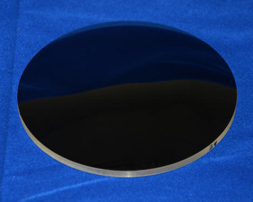
Silicon (Si) lenses manufactured using optical grade silicon are competent for light collimation, direction, and manipulation in the IR spectrum. There are two kinds of silicon, Czochralski Si, used for the 3-5μm MWIR range, and Float Zone Si, used for the 8-12μm LWIR range. It has a low density of half the magnitude of Ge or ZnSe, thus Si lens is ideal for weight-sensitive applications. Silicon is also harder and less brittle than germanium, with the additional virtue of chemical resistance and low cost.
Curves:
1. Transmission Curve of Silicon with No Coating
![]()
2. Transmission Curve of Silicon Lens with AR/AR Coating at 3-5μm
![]()