| Specification | |
| Top Functional Layer | |
| Diameter | 3, 4, 6 inches, or other custom diameters |
| Orientation | Y-42, Y-46.3, Z, etc. |
| Material | LiTaO3 |
| Thickness | 300-900 nm |
| Isolation Layer | |
| Material | SiO2 |
| Thickness | 300-4000nm |
| Substrate | |
| Material | Si |
| Thickness | 400-500μm |
Modules or Types:
| Single-crystal Lithium Tantalate Thin Film |
| SiO2 |
| Silicon Substrates |
Lithium Tantalate On Insulator (LTOI) represents a cutting-edge platform in the field of integrated photonics and electronics, offering a fusion of the unique properties of lithium tantalate (LiTaO3) with the scalabilities and compatibilities of insulating substrates. Lithium tantalate crystal belongs to the trigonal system, 3m point group, and r3c space group. Due to its anisotropic lattice structure, different orientations have different application fields. For example, in the area of Radio Frequency (RF) front-end devices, orientations of lithium tantalate wafers majorly include 38-degree y-x cut, 42-degree y-x cut, 50-degree y-x cut, etc. In the pyroelectric field, the most prevalent orientation of LiTaO wafers is z-cut.
Lithium tantalate (LiTaO3) is renowned for its exceptional nonlinear-optical, piezoelectric, and nonlinear optical properties. Leveraging these inherent characteristics, LTOI enables the integration of LiTaO3-based devices into silicon photonics platforms. Its high electro-optic coefficient facilitates efficient modulation of light signals, essential for high-speed data communication devices. Thin-film lithium tantalate possesses a higher laser-induced damage thresholds and photorefractive damage threshold than LNOI. These exceptional properties make lithium tantalate on insulator (LTOI) a promising material platform for high-power and short-wavelength (down to the UV) integrated photonic devices.
With excellent piezoelectric properties, LTOI can convert, mechanical energies into electrical energies with high efficiencies, rendering them an attractive candidate for high-performance RF filters, mobile phones, and wireless communication. Integrating lithium tantalate and silicon-based substrates to fabricate silicon-based lithium tantalate piezoelectric thin film (Lithium Tantalate On Insulator, LTOI) will grant access to a new path to manufacture RF filters with high q value, low tcf, superior Fs steadiness, Ke^2>10%, excellent thermal conduction, and low production cost. In addition, LiTaO3 Thin films are also expected to stimulate the utilization of SAW modes with higher acoustic velocities, which is helpful in increasing the operating frequencies of filters, and of great significance in meeting the requirement of spectrum expansion posed by the 5G technologies.
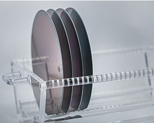
Hangzhou Shalom EO offers custom Lithium Tantalate On Insulator (LTOI) consisting of a LiTaO3 thin film on a silicon substrate. Various cut directions are available, the thickness of the functional LiTaO3 layer is 300-900nm, and SiO2 insulation layers are optional.