| Code | Size | Thickness | Orientation | Surface Finish | Unit Price | Delivery | Cart |
|---|---|---|---|---|---|---|---|
| 645-001 | 5x5mm | 0.5mm | <100> | SSP | Inquire | 2 weeks | |
| 645-002 | 5x5mm | 0.5mm | <100> | DSP | Inquire | 2 weeks | |
| 645-004 | 5x5mm | 0.5mm | <111> | SSP | Inquire | 2 weeks | |
| 645-005 | 10x10mm | 0.5mm | <100> | SSP | Inquire | 2 weeks | |
| 645-006 | 10x10mm | 0.5mm | <100> | DSP | Inquire | 2 weeks | |
| 645-007 | 10x10mm | 0.5mm | <110> | SSP | Inquire | 2 weeks | |
| 645-008 | 10x10mm | 0.5mm | <111> | SSP | Inquire | 2 weeks | |
| 645-009 | φ25.4mm | 0.5mm | <100> | SSP | Inquire | 2 weeks | |
| 645-010 | φ25.4mm | 0.5mm | <100> | DSP | Inquire | 2 weeks | |
| 645-011 | Φ50.8mm | 0.5mm | <100> | SSP | Inquire | 2 weeks | |
| 645-012 | Φ50.8mm | 0.5mm | <100> | DSP | Inquire | 2 weeks | |
| 645-013 | Φ76.2mm | 0.5mm | <100> | SSP | Inquire | Inquire | |
| 645-014 | Φ76.2mm | 0.5mm | <100> | DSP | Inquire | Inquire |
LaAlO3 (Lanthanum aluminate) single crystal with a perovskite crystal structure, has a good lattice match to multiple materials with a similar perovskite structure. Its wide bandgap, thermal stabilities, and low dielectric loss make it excellent for applications in electronics of high frequencies, optics, and indispensable platforms for the epitaxial growth and research of thin films and heterostructures. Various materials can be grown on LaAlO2, including complex oxides, high-temperature superconductors, magnetic materials, and multiferroics. LaAlO3 exhibits a high dielectric constant, making it useful in capacitor applications.
Hangzhou Shalom EO provides stock epi-ready LaAlO3 wafers and custom LaAlO3 wafers upon request.
Applications of LaAlO3 Substrates:
Common Specifications:
| Material | LaAlO3 crystals | Orientation | <100>,<110>,<111> |
| Orientation Error | ±0.5° | Maximum Diameter | 3 inches |
| Typical Thickness | 0.5mm, 1.0mm | Thickness Tolerance | ±0.05mm |
| Size Tolerance | ±0.1mm | Surface Finish | SSP or DSP |
| Roughness | Ra<0.5nm | Cleanness and Package | class 1000 clean room, class 100 bags |
Curves:
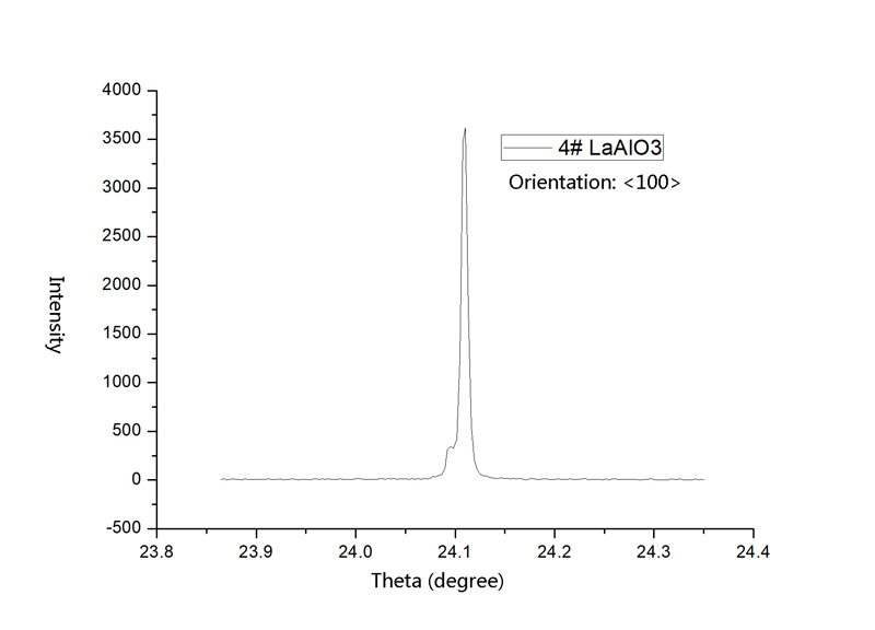
1)Typical X-Ray Diffraction (XRD) Curve of LaAlO3 <100> Crystals Substrates

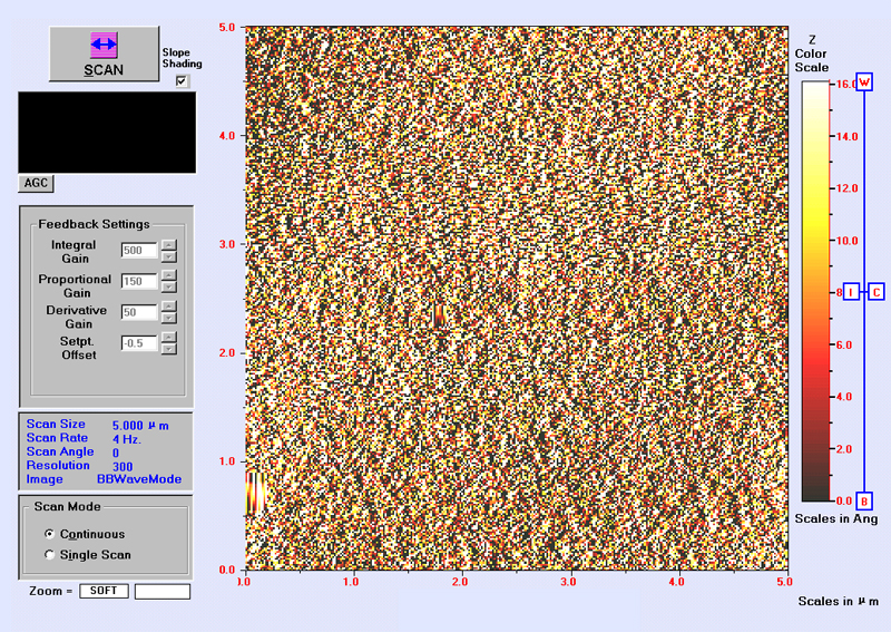
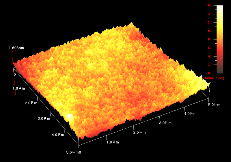
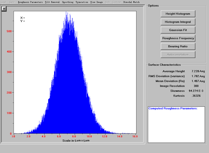
2) Typical Surface Roughness of substrate LaAlO3 <100> and <001> measured by Atomic Force Microscope (AFM) in 5μm x 5μm Scale


