01.jpg)
| Code | Size | Thickness | Orientation | Surface Finish | Unit Price | Delivery | Cart |
|---|---|---|---|---|---|---|---|
| 641-001 | 5x5mm | 0.5mm | <100> | SSP | Inquire | 2 weeks | |
| 641-002 | 5x5mm | 0.5mm | <100> | DSP | Inquire | 2 weeks | |
| 641-003 | 5x5mm | 0.5mm | <110> | SSP | Inquire | 2 weeks | |
| 641-004 | 5x5mm | 0.5mm | <111> | SSP | Inquire | 2 weeks | |
| 641-005 | 10x10mm | 0.5mm | <100> | SSP | Inquire | 2 weeks | |
| 641-006 | 10x10mm | 0.5mm | <100> | DSP | Inquire | 2 weeks | |
| 641-007 | 10x10mm | 0.5mm | <110> | SSP | Inquire | 2 weeks | |
| 641-008 | 10x10mm | 0.5mm | <111> | SSP | Inquire | 2 weeks | |
| 641-009 | Φ12.7mm | 0.5mm | <100> | SSP | Inquire | 2 weeks | |
| 641-010 | Φ12.7mm | 0.5mm | <100> | DSP | Inquire | 2 weeks | |
| 641-011 | Φ25.4mm | 0.5mm | <100> | SSP | Inquire | 2 weeks | |
| 641-012 | Φ25.4mm | 0.5mm | <100> | DSP | Inquire | 2 weeks | |
| 641-013 | Φ50.8mm | 0.5mm | <100> | SSP | Inquire | 2 weeks | |
| 641-014 | Φ50.8mm | 0.5mm | <100> | DSP | Inquire | Inquire |
MgO (Magnesium Oxide Crystals), due to its low dielectric constant and minimal microwave band loss, along with the availability of large-sized wafers (up to 2 inches in diameter and larger), has emerged as a crucial industrial material for High-Temperature Superconductor (HTS) thin monocrystalline wafers. MgO serves as an exceptional single-crystal substrate catering to various thin film growth tasks including Ferro-magnetic, Photo-electronic, semiconductor, and high-temperature superconductor films. Its utility extends to III to V element research, exploring epitaxial effects on polymer crystallization, and even for depositing ferroelectric coatings on its substrates. Moreover, MgO wafers find increasing applications in Plasma Display Panel (PDP) technology.
Hangzhou Shalom EO provides both stocked standard MgO wafers and customized wafers.
Common Specifications:
| Material | MgO crystals | Orientation | <100>,<110>,<111> |
| Orientation Error | ±0.5° | Maximum Size | 50x50mm |
| Typical Thickness | 0.5mm, 1.0mm | Thickness Tolerance | ±0.05mm |
| Size Tolerance | ±0.1mm | Surface Finish | SSP or DSP |
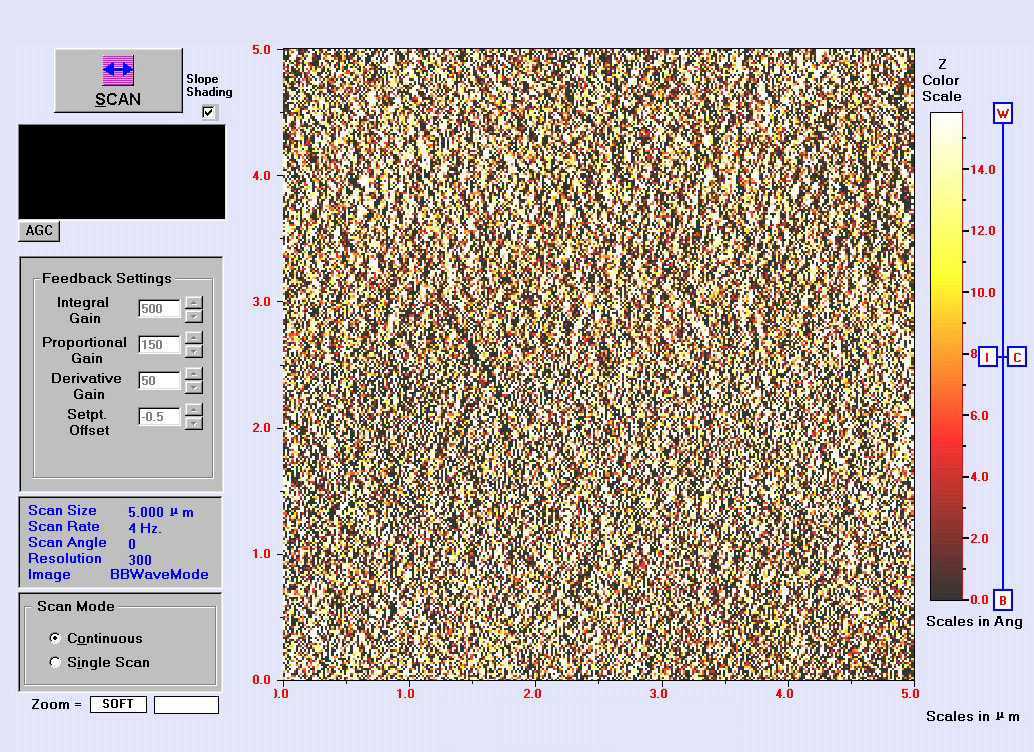
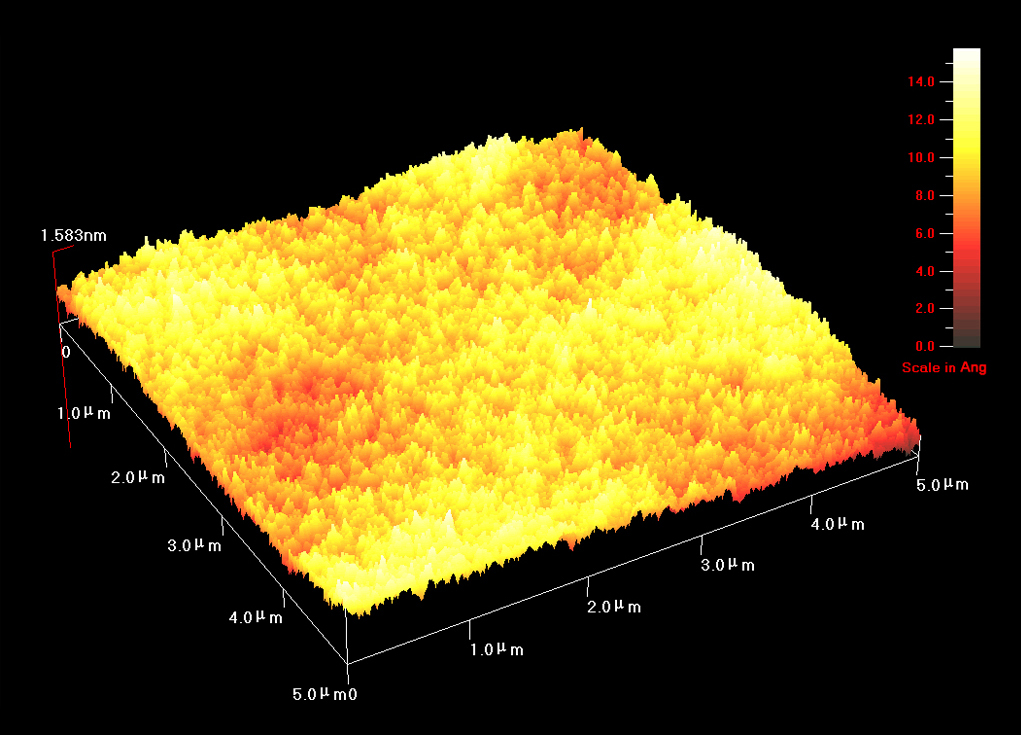
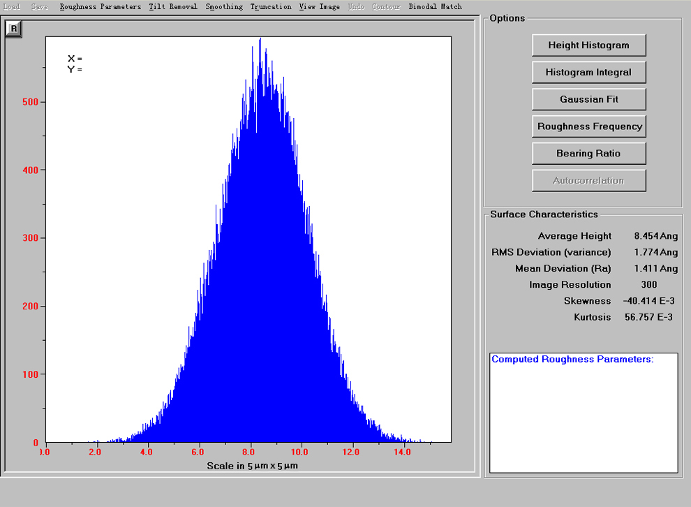
| Roughness | Ra<0.5nm | Cleaness and Package | 1000 grade clean room, 100 grade bags |
MgO Properties:
| Growth Method | Special Arc Melting | Crystallographic Structure | Cubic a = 4.13 Å |
| Twinning Structure | Twin free | Orientation | <100>, <110>, <111> |
| Colour | Colourless | Transmission Range | 0.2 to 8 µm |
| Density | 3. 585 g/cm3 | Melting Point | 2780 +/- 20 °C |
| Thermal Expansion Coefficient | 11.2 * 10-6 K-1 | Dielectric Constant | 9.65 |
| Specific Resistivity | > 1017Ohm/cm |
Curves:
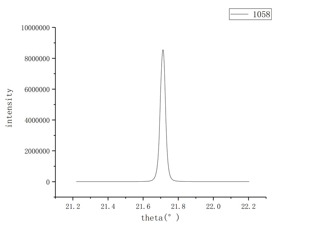
1)Typical X-Ray Diffraction (XRD) Curve of MgO <100> Crystals Substrates

2) Typical Surface Roughness of MgO substrate <100> and <010> measured by Atomic Force Microscope (AFM) in 5μm x 5μm Scale


