| Code | Size | Thickness | Orientation | Surface Finish | Unit Price | Delivery | Cart |
|---|---|---|---|---|---|---|---|
| 645-001 | 5x5mm | 0.5mm | <100> | SSP | Inquire | 2 weeks | |
| 645-002 | 5x5mm | 0.5mm | <100> | DSP | Inquire | 2 weeks | |
| 645-004 | 5x5mm | 0.5mm | <111> | SSP | Inquire | 2 weeks | |
| 645-005 | 10x10mm | 0.5mm | <100> | SSP | Inquire | 2 weeks | |
| 645-006 | 10x10mm | 0.5mm | <100> | DSP | Inquire | 2 weeks | |
| 645-007 | 10x10mm | 0.5mm | <110> | SSP | Inquire | 2 weeks | |
| 645-008 | 10x10mm | 0.5mm | <111> | SSP | Inquire | 2 weeks | |
| 645-009 | φ25.4mm | 0.5mm | <100> | SSP | Inquire | 2 weeks | |
| 645-010 | φ25.4mm | 0.5mm | <100> | DSP | Inquire | 2 weeks | |
| 645-011 | Φ50.8mm | 0.5mm | <100> | SSP | Inquire | 2 weeks | |
| 645-012 | Φ50.8mm | 0.5mm | <100> | DSP | Inquire | 2 weeks | |
| 645-013 | Φ76.2mm | 0.5mm | <100> | SSP | Inquire | Inquire | |
| 645-014 | Φ76.2mm | 0.5mm | <100> | DSP | Inquire | Inquire |
LaAlO3 (Lanthanum aluminate) single crystal has a good lattice match to many materials with perovskite structure. It is an excellent substrate for epitaxial growth of high temperature superconductors (HTS), magnetic and ferro-electric thin films. The dielectric properties of LaAlO3 crystal are well suitable for low loss microwave and dielectric resonance applications.
Hangzhou Shalom EO not only provides the stocked standard epi-ready LaAlO3 wafers, but also the custom type wafers upon request.
Common Specifications:
| Material | LaAlO3 crystals | Orientation | <100>,<110> ,<111> |
| Orientation Error | ±0.5° | Maximum Diameter | 3 inches |
| Typical Thickness | 0.5mm, 1.0mm | Thickness Tolerance | ±0.05mm |
| Size Tolerance | ±0.1mm | Surface Finish | SSP or DSP |
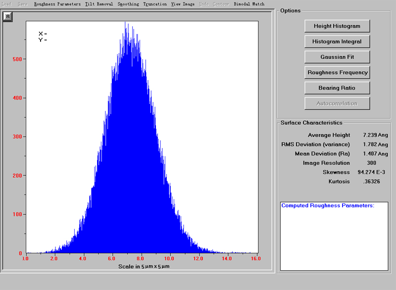
| Roughness | Ra<0.5nm | Cleaness and Package | 1000 grade clean room, 100 grade bags |
Curves:
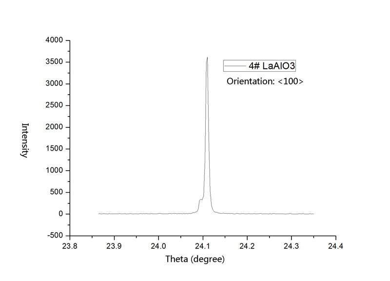
1)Typical X-Ray Diffraction (XRD) Curve of LaAlO3 <100> Crystals Substrates

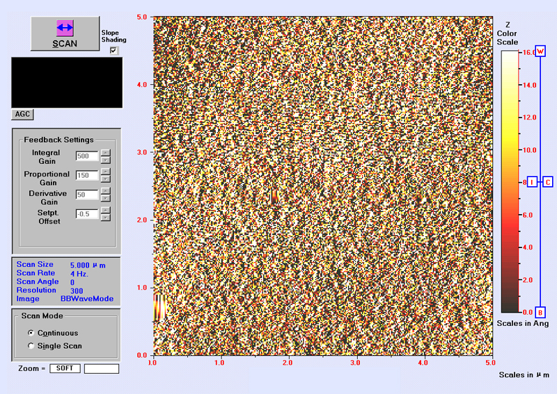
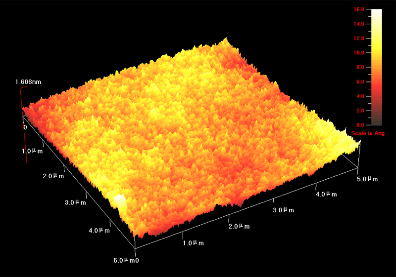
2) Typical Surface Roughness of substrate LaAlO3 <100> and <001> measured by Atomic Force Microscope (AFM) in 5μm x 5μm Scale


