01.jpg)
| Code | Size | Thickness | Orientation | Surface Finish | Unit Price | Delivery | Cart |
|---|---|---|---|---|---|---|---|
| 6506-001 | 5x5mm | 0.5mm | <100> | SSP | Inquire | 2 weeks | |
| 6506-002 | 5x5mm | 0.5mm | <110> | SSP | Inquire | 2 weeks | |
| 6506-003 | 5x5mm | 0.5mm | <111> | SSP | Inquire | 2 weeks | |
| 6506-004 | 10x10mm | 0.5mm | <100> | SSP | Inquire | 2 weeks | |
| 6506-005 | 10x10mm | 0.5mm | <110> | SSP | Inquire | 2 weeks | |
| 6506-006 | 10x10mm | 0.5mm | <111> | SSP | Inquire | 2 weeks | |
| 6506-007 | Φ12.7mm | 0.5mm | <111> | SSP | Inquire | 2 weeks | |
| 6506-008 | Φ12.7mm | 0.5mm | <111> | DSP | Inquire | 2 weeks | |
| 6506-009 | Φ25.4mm | 0.5mm | <111> | SSP | Inquire | 2 weeks | |
| 6506-010 | φ25.4mm | 0.5mm | <111> | DSP | Inquire | 2 weeks | |
| 6506-011 | φ50.8mm | 0.5mm | <111> | SSP | Inquire | 2 weeks | |
| 6506-012 | φ50.8mm | 0.5mm | <111> | DSP | Inquire | 2 weeks | |
| 6506-013 | φ76.2mm | 0.5mm | <111> | SSP | Inquire | Inquire | |
| 6506-014 | φ76.2mm | 0.5mm | <111> | DSP | Inquire | Inquire |
Gadolinium Gallium Garnet (GGG) single crystal is a material with exceptional magneto-optical properties, low dielectric loss, and high thermal conduction which make it promising for use in the fabrication of various optical magneto-optical components as well as for epitaxial growth of microwave elements and high-temperature superconductors. GGG substrates can be incorporated into infrared optical isolator (operating from 1.3μm to 1.5μm), which comprises YIG or BIG film deposited on the Gadolinium Gallium Garnet (GGG) substrate combined with birefringence parts. GGG substrates enable the fabrication of high-performance optoelectronic devices such as lasers, light-emitting diodes (LEDs), and photodetectors.
Hangzhou Shalom EO provides standard epi-ready GGG substrates and wafers, custom GGG wafers are also available upon request.
Common Specifications:
| Material | GGG single crystals | Orientation | <100>,<110>,<111> |
| Orientation Error | ±0.5° | Maximum Diameter | 4 inches |
| Typical Thickness | 0.5mm,1.0mm | Size Tolerance | ±0.05mm |
| Size Tolerance | ±0.1mm | Surface Finish | SSP or DSP |
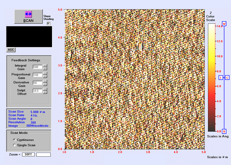
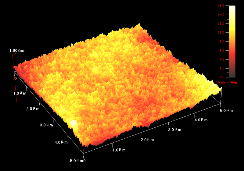
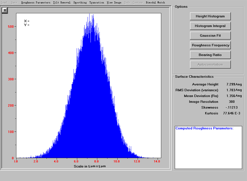
| Roughness | Ra<0.5nm | Cleanness and Package | class1000 clean room, class 100 bags |
Physical Properties:
| Density, g/cm3 (20°C) | 7.08 | Type of Materials | Single crystal |
| Crystal Structure | cubic | Lattice Parameter, A | 12.383 |
| Melting Point (°C) | 1750 | Thermal Conductivity, W x cm-1 x °K-1 | 7.05 |
| Thermal Expansion, 1/°C | 8.2x10⁻⁶ | Dielectric Constant | 30 |
| Dielectric Loss Tangent, at 10GHz | 0.15 | Mohs Hardness | 7.5 |
Curves:
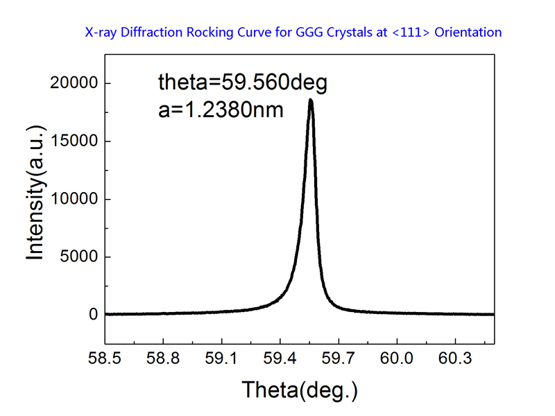
1)Typical X-Ray Diffraction (XRD) Curve of GGG Crystals Substrates and Wafers
2) Typical Surface Roughness of GGG substrate <111> measured by Atomic Force Microscope (AFM) in 5μm x 5μm Scale