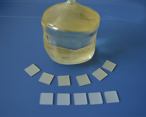
| Code | Size | Thickness | Orientation | Surface Finish | Unit Price | Delivery | Cart |
|---|---|---|---|---|---|---|---|
| 643-001 | 5x5mm | 0.5mm | <100> | SSP | Inquire | 2 weeks | |
| 643-002 | 5x5mm | 0.5mm | <100> | DSP | Inquire | 2 weeks | |
| 643-003 | 5x5mm | 0.5mm | <110> | SSP | Inquire | 2 weeks | |
| 643-004 | 5x5mm | 0.5mm | <111> | SSP | Inquire | 2 weeks | |
| 643-005 | 10x10mm | 0.5mm | <100> | SSP | Inquire | 2 weeks | |
| 643-006 | 10x10mm | 0.5mm | <100> | DSP | Inquire | 2 weeks | |
| 643-007 | 10x10mm | 0.5mm | <110> | SSP | Inquire | 2 weeks | |
| 643-008 | 10x10mm | 0.5mm | <111> | SSP | Inquire | 2 weeks | |
| 643-009 | Φ12.7mm | 0.5mm | <100> | SSP | Inquire | 2 weeks | |
| 643-010 | Φ12.7mm | 0.5mm | <100> | DSP | Inquire | 2 weeks | |
| 643-011 | Φ25.4mm | 0.5mm | <100> | SSP | Inquire | 2 weeks | |
| 643-012 | Φ25.4mm | 0.5mm | <100> | DSP | Inquire | 2 weeks | |
| 643-013 | Φ50.8mm | 0.5mm | <100> | SSP | Inquire | Inquire | |
| 643-014 | Φ50.8mm | 0.5mm | <100> | DSP | Inquire | Inquire |
LSAT - Lanthanum Strontium Aluminum Tantalum Oxide or (La,Sr)(Al,Ta)O3 is a mixed perovskite structure crystal, LSAT substrates are often used for epitaxial thin film growth in ferroelectric and high-temperature superconductor (HTS) devices. LSAT is a hard, optically transparent oxide of the elements lanthanum, aluminum, strontium, and tantalum, LSAT wafers are popular for epitaxial oxides and their heterostructures, often in the study of electron correlation phenomena. Typical materials grown on LSAT substrates include strontium titanate (SrTiO3), cuprate superconductors (such as YBCO), iron-based superconductors (iron-pnictides), rare-earth manganite, rare-earth nickelates, and others. Semiconductors such as gallium nitride can also be grown on LSAT.
Hangzhou Shalom EO provides both stocked standard LSAT wafers and customized wafers.
Common Specifications:
| Material | LSAT crystals | Orientation | <100>,<110>,<111> |
| Orientation Error | ±0.5° | Maximum Diameter | 2 inches |
| Typical Thickness | 0.5mm, 1.0mm | Thickness Tolerance | ±0.05mm |
| Size Tolerance | ±0.1mm | Surface Finish | SSP or DSP |
| Roughness | Ra<0.5nm | Cleaness and Package | 1000 grade clean room, 100 grade bags |
Basic Properties:
| Growth Method | Czochralski method | Crystal Structure | M3 |
| Unit Cell Constant | a=3.868 Å | Melt Point(℃) | 1840 |
| Density | 6.74(g/cm3) | Hardness | 6.5(mohs) |
| Dielectric Constants | 22 | Thermal Expansion | 10 x 10-6 /K |